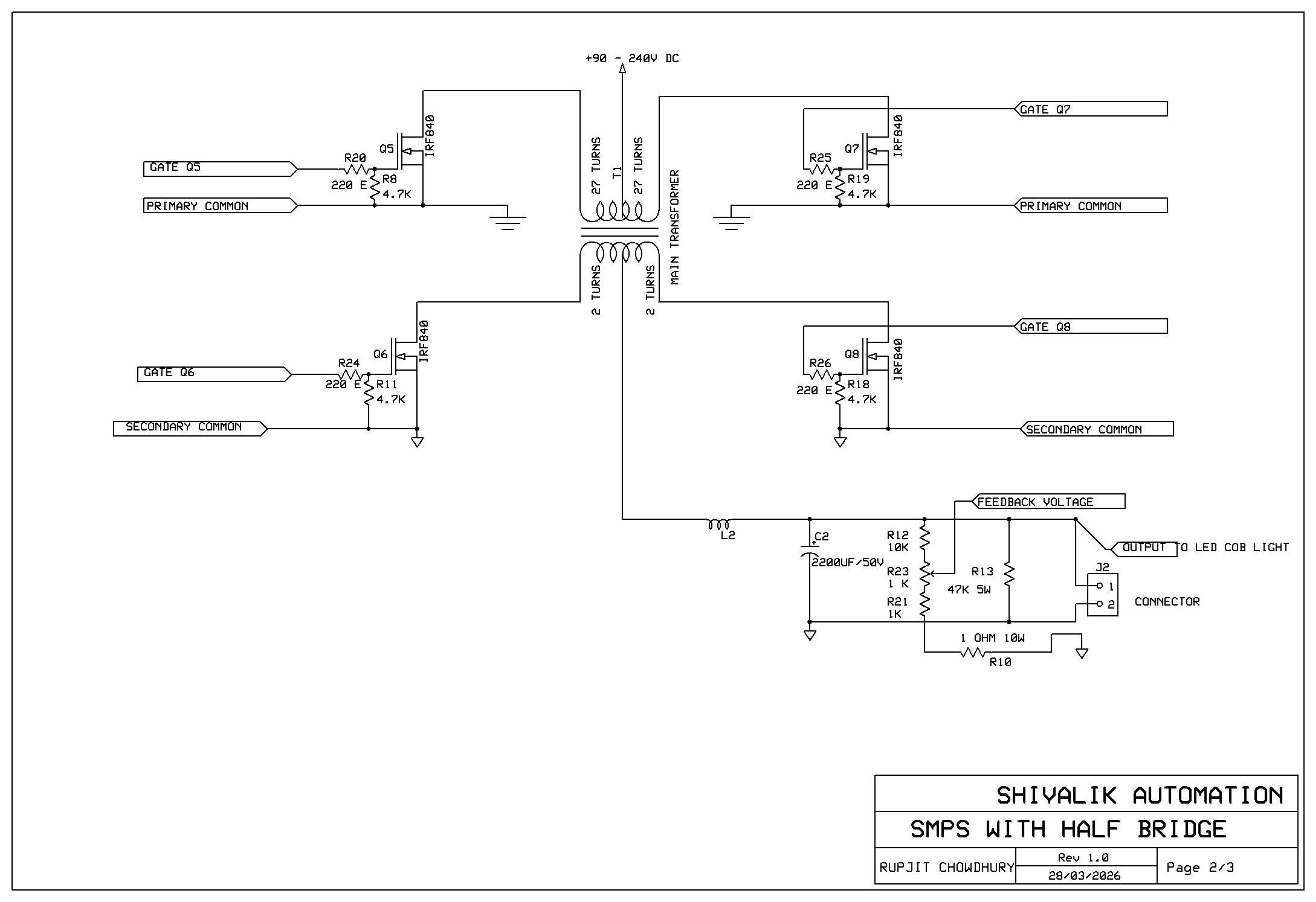
Half bridge SMPS 110V - 220V AC to 27V DC. Power stage input and output are mosfets IRF840.No schottkey rectifieres used
Introduction
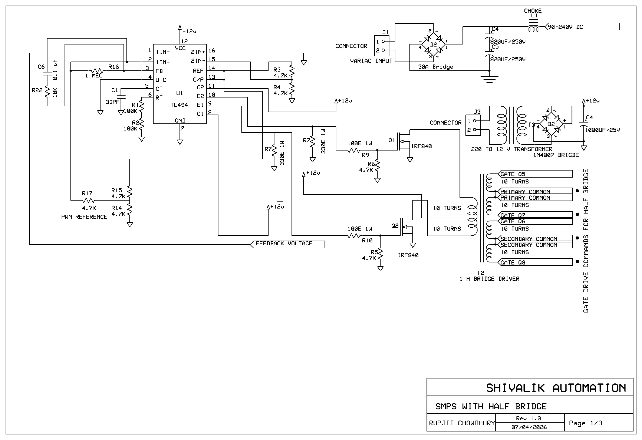
In this circuit design we are going to make a SMPS using half bridge configuration in the primary side of the power transformer. The secondary side
of the power transformer is a center tapped winding and is connected to another half bridge configuration. The SMPS is designed on IC TL494 which
is the PWM oscillator ic. The operating frequency of the circuit is around 53 Khz. There are two transformers used. One is the driver transformer
and the other is the power transformer. The driver transformer controls two mosfets connercted in primary side of power transformer in half bridge configuration.
Two other mosfets are connected in secondary side of the power transformer in another half bridge configuration. We are not using schottkey diode in
transformer secondary for DC generation. The polarity of the gate firing signals is discussed in the design.
Description
The Oscillator with feedback: The circuit is controlled by U1 i.e. IC TL494. This is the main PWM controller IC. R1+R2 in parallel
to C1 makes a frequency of 53Khz. Pin 8 and Pin 11 are collector pins and they are pulled up to +12V DC. The IC U1 is also powered by +12V DC. Pin 9 an 10 are emitter pins of IC TL494 and they drive
the driver transformer T2. The DC output voltage is fed to voltage divider R12, R21 and R23 and R23 output is fed the Pin 1 of IC TL494 for PWM
voltage control.
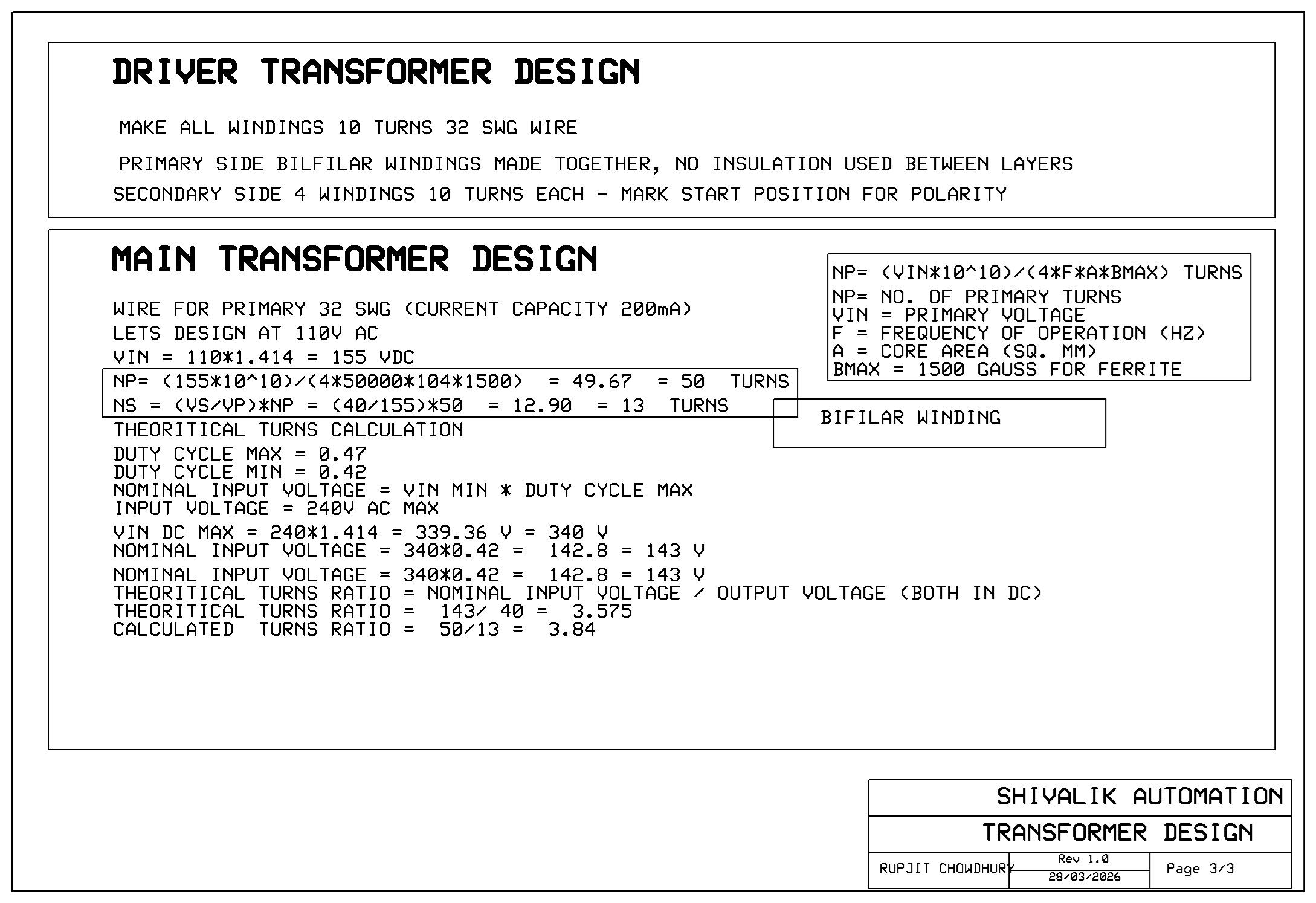
Driver stage: The driver transformer T2 primary side is a bifilar winding 10 turns each. Q1 and Q2 are mosfets IRF840 that controls driver transformer in half
bridge mode. R5 and R6 are connected between gate and emitter of mosfets Q1 and Q2. The secondary side of the driver transformer has two bifilar windings
of 10 turns each. The start and finish point of these secondary windings are to be marked as these will be the polarity for the next stage. Coil
start has a black dot that indicates start end of each winding. The secondary windings are therefore two sets of similar windings that control the
power stage.
Half bridge power stage: The Half bridge is made of two mosfets Q5, Q7 in primary side of the power transformer and Q6, Q8 in secondary side of power transformer. These mosfets are triggered with correct polarity at their respective gates. The driver transformer windings are fed between gate and emitter of each mosfet. Also a 4.7K resistor is used between gate and emitter R8, R11, R18, R19. Also there are current limiting resistors R20, R24, R25 and R26 of 220 ohm each. Note that the DC rectification in
the secondary side is having no Schottky diode, The mosfets Q6 and Q8 are used as rectifiers. Secondary side of transformer T1 common terminal is positive
rail and is connected to choke L2 of 20 turns wire on ferrite ring. The filter capacitor C2 finally filters and generates the output. This is fed to voltage divider R12, R21 and R23 and R23 output is fed the Pin 1 of IC TL494 for PWM voltage control.
Circuit Diagram
Bill of Materials
Click here for bill of materials
Software -- Nil
Results
Conclusion
The circuit is built as a reference design and used to drive LED module. Please watch the performance on the youtube link provided.